This post introduces Compute Express Link (CXL), an open, cache-coherent interconnect standard for attaching memory and accelerators to processors. CXL represents the most significant architectural change to the server memory subsystem since the introduction of integrated memory controllers: it decouples memory capacity and bandwidth from the processor’s DDR channel count, enabling memory expansion, tiering, and rack-scale pooling.
What is CXL?
CXL is an open industry-standard interconnect layered on the PCIe physical layer. A CXL device is electrically and mechanically a PCIe device: it occupies a standard slot and uses PCIe signaling (PCIe 5.0 for CXL 1.1 and 2.0; PCIe 6.0 for CXL 3.x). CXL differs from PCIe not in its physical layer but in its transaction semantics.
A CXL link multiplexes three sub-protocols:
| Protocol | Purpose |
|---|---|
| CXL.io | Device discovery, configuration, and DMA; semantically equivalent to PCIe |
| CXL.cache | Permits a device to coherently cache host memory |
| CXL.mem | Permits the host to access device-attached memory via load/store instructions |
The salient property of CXL is hardware-managed cache coherence. Under PCIe, host and device cannot transparently share memory: software must orchestrate explicit DMA transfers and cache flushes. Under CXL, a processor may issue an ordinary load or store to an address backed by device-attached memory, and the coherence protocol maintains consistency with processor caches, exactly as it does for socket-attached DIMMs.
The specification composes these sub-protocols into three device types:
- Type 1 (CXL.io + CXL.cache): accelerators without device-attached memory (e.g., SmartNICs) that coherently cache host memory.
- Type 2 (all three protocols): accelerators with device-attached memory (e.g., GPUs), where host and device require mutual coherent access.
- Type 3 (CXL.io + CXL.mem): memory expanders, devices whose sole function is to extend system memory capacity and bandwidth. Type 3 devices account for the majority of current industrial deployment and are the primary focus of this series.
To system software, the memory of a Type 3 device is exposed as an additional physical address range, conventionally enumerated as a CPU-less NUMA node. The operating system can therefore manage it with existing NUMA mechanisms: allocation policies, page migration, and memory tiering.
How does CXL memory differ from DRAM?
A CXL memory expander is populated with commodity DRAM. The distinction between “DRAM” and “CXL memory” is therefore not one of memory media but of the access path between the processor and that media.
The DDR path versus the CXL path
Conventional DRAM resides on DIMMs attached to DDR channels wired directly to the processor’s integrated memory controller. The DDR interface is a wide, parallel, synchronous bus: a single DDR5 channel dedicates approximately 300 package pins to data, address, command, and clock signals, all operating in lockstep at a fixed frequency.
A CXL expander instead resides behind a narrow, serial link. A x16 CXL link requires approximately 80 package pins (16 differential transmit pairs, 16 receive pairs, clocking, and sideband). Accesses are packetized: a load is encoded as a CXL.mem request flit, traverses the link, is decoded by the controller on the device, is serviced from the device’s DRAM, and returns as a response flit.
This difference in access path determines the performance and scaling characteristics of the two technologies.
Latency. A local DDR5 access completes in approximately 80–100 ns. A CXL access incurs additional link-traversal and protocol overhead at both endpoints, yielding approximately 170–250 ns for directly attached devices—comparable to a remote-socket access in a two-socket NUMA system, or roughly 2–2.5× local DRAM latency. CXL memory remains orders of magnitude faster than storage (NVMe access latency is on the order of 10 µs) but is measurably slower than local DRAM. Consequently, CXL memory is architecturally positioned as a distinct memory tier rather than as a substitute for locally attached DRAM.
Bandwidth. A single DDR5-5600 channel provides approximately 44 GB/s; a x16 CXL 2.0 link (PCIe 5.0) provides approximately 64 GB/s per direction. Per-link bandwidth is thus comparable. The important distinction is that CXL bandwidth is additive: it is drawn from the PCIe lane budget rather than the DDR channel budget, so attaching CXL memory increases aggregate system bandwidth rather than contending for existing DDR bandwidth.
Capacity scaling. Here the two technologies diverge fundamentally, and the root cause is the processor’s pin budget.
The pin constraint: why DIMM slots do not scale
A processor package provides a fixed number of pins, and parallel DDR interfaces consume them at a high rate: each additional channel costs approximately 300 pins, and signal-integrity constraints limit each channel to at most two DIMMs (frequently one at the highest transfer rates). Contemporary server processors therefore provide 8–12 DDR channels, already a substantial fraction of the total pin budget. Once all DIMM slots are populated, capacity can be increased only by adopting a larger processor SKU or an additional socket.
CXL relaxes this constraint in two ways. First, serial signaling is approximately 4× more pin-efficient per unit bandwidth than parallel DDR. Second, and more importantly, CXL links are switchable: a single x16 root port can fan out through a switch to many memory devices. DDR channels admit no switching; their topology is fixed at board design time.
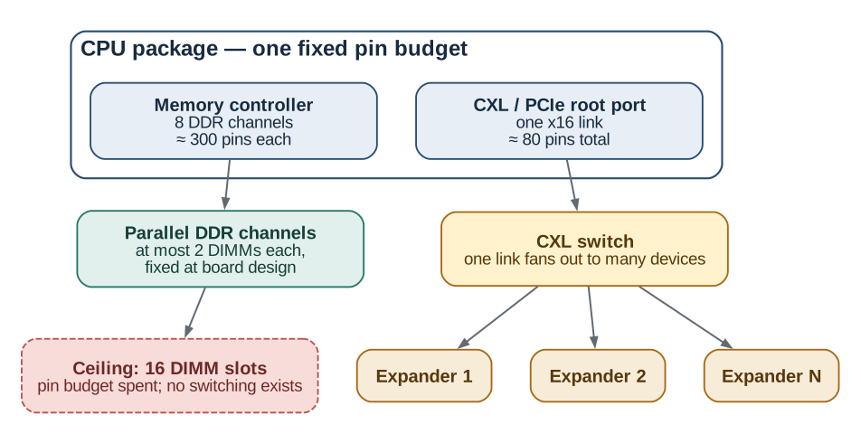
The diagram illustrates the essential asymmetry. The DDR topology is terminal: each channel represents a large, fixed pin investment, and per-channel fan-out is bounded at two DIMMs by electrical constraints. The CXL topology is a tree: one pin-inexpensive serial link reaches a switch, and the switch fans out to an arbitrary number of memory devices. CXL 3.x further generalizes the tree to multi-level switching, i.e., a memory fabric.
Summary of the differences
| DDR-attached DRAM | CXL-attached memory | |
|---|---|---|
| Interface | Parallel bus, ~300 pins/channel | Serial lanes, ~80 pins per x16 link |
| Access latency | ~80–100 ns | ~170–250 ns (comparable to a remote NUMA access) |
| Topology | Point-to-point, fixed at board design | Switchable; fabric-capable in CXL 3.x |
| Capacity ceiling | 8–12 channels × 2 DIMMs | Bounded by lane count × switch fan-out; substantially higher |
| Reconfigurability | DIMM population fixed at boot | Hot-plug and dynamic capacity (CXL 2.0+) |
| Media flexibility | DRAM only | DRAM today; alternative or hybrid media behind the same interface |
The final row merits emphasis. Because CXL abstracts the memory media behind a load/store protocol, a Type 3 device may internally employ DRAM, a DRAM–flash hybrid, or a future memory technology without any change visible to the processor. The DDR interface binds a processor generation to a specific memory technology; CXL removes that binding.
Potential use cases
Memory capacity expansion. A server whose DIMM slots are fully populated can extend capacity by terabytes via CXL expanders. For capacity-bound workloads—in-memory databases and key-value stores such as SAP HANA, Redis, and Memcached—tolerating an additional ~100 ns on a fraction of accesses is substantially cheaper than scaling out to additional servers.
Memory tiering. The operating system places frequently accessed pages in local DRAM and demotes infrequently accessed pages to CXL memory, promoting them upon reuse. Linux already provides this mechanism through its memory-tiering and transparent page placement infrastructure. Published measurements from hyperscale operators indicate that a large fraction of datacenter memory is cold at any given time, so tiering recovers significant cost at modest performance impact.
Memory pooling and disaggregation. Studies from Microsoft Azure and Google report that a substantial fraction of provisioned DRAM is stranded: reserved by virtual machines but never touched, or unallocatable after a host’s cores are exhausted. With CXL 2.0 switching, a rack can maintain a shared memory pool that is dynamically assigned to hosts on demand and reclaimed thereafter. Memory thereby becomes a rack-level resource, as storage already is, rather than a resource confined to individual hosts. This use case carries the largest economic significance.
Coherent accelerators. Type 1 and Type 2 devices allow GPUs, NICs, and domain-specific accelerators to share data structures with the host without explicit copies: a pointer is valid on both sides of the link.
Bandwidth expansion. Bandwidth-bound workloads—embedding-dominated recommendation models and KV-cache-dominated LLM inference among them—can interleave allocations across DDR and CXL simultaneously, exploiting CXL links as additional bandwidth rather than additional capacity.
The future of CXL
CXL has consolidated the coherent-interconnect landscape: the competing OpenCAPI, Gen-Z, and CCIX efforts have transferred their assets to the CXL Consortium. All major server processor vendors now ship CXL support—Intel since Sapphire Rapids, AMD since Genoa, alongside the Arm server ecosystem.
The specification roadmap proceeds as follows:
- CXL 2.0 (shipping): single-level switching, memory pooling across up to 16 hosts, and hot-plug.
- CXL 3.x (arriving with PCIe 6.0 platforms): doubled per-link bandwidth at unchanged latency, multi-level switching, fabrics spanning hundreds of nodes, peer-to-peer transfers between devices, and hardware-coherent shared memory regions mapped simultaneously by multiple hosts. The last capability enables system designs in which, for example, the nodes of a distributed database operate over a single coherent memory image.
The plausible near-term trajectory is tiered, pooled memory as the default server organization: a modest complement of low-latency local DDR per socket, backed by a large switch-attached CXL pool shared across the rack. Whether the more ambitious endpoint—full rack-scale disaggregation, in which compute and memory scale independently—is reached on schedule depends chiefly on how effectively system software (kernels, hypervisors, and databases) can tolerate the additional 100–150 ns of access latency.
That software question—how Linux discovers, onlines, tiers, and migrates CXL memory—is the subject of the next post in this series.